
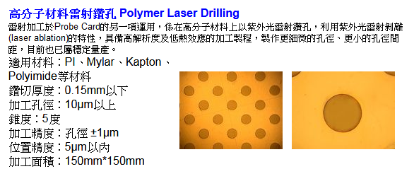
Wafer probe card has multiple isolation layers on which thousands of fine holes should be drilled for probe pin to go through. This stage is used to move the isolation layer to the accurate position and the holes are drilled by laser beam.
Stage specification
| ITEM | X axis (up) | Yaxis(down) | Z axis | |
| Stroke | Effective (mm) | 150 | 150 | |
| Maximal (mm) | 160 | 160 | ||
| Resolution (um) | 0.05 | 0.05 | ||
| Straightness (um) | <1 | <1 | ||
| Flatness (um) | <5 | <5 | ||
| XYZ squareness (um) | <2 | |||
| Repeatability (um) | +/- 0.1 | +/- 0.1 | ||
| Accuracy (um)
(with laser calibration) |
< 1 | < 1 | ||
| Maximal speed (m/sec) | 0.8 | 0.8 | ||
| Maximal Acc. (G) | 2 | 2 | ||
- The up axis and down axis are stacked with a very low profile design. The distance between working surface of up axis and linear guide mounting surface of down axis is only 100 mm.
- Wide span design of down axis together with driven by dual linear motors eliminates resonance in yaw direction due to gravity center change of up axis.
- The stage employees a bottom base made of cast iron to absorb vibration.
- Built-in cable chain and fully covered bellow to improve protection grade.
- Ultra-low cogging force linear motors are employed.